Research Journal Articles
My research articles delve into advanced semiconductor devices, IoT systems, and sustainable technologies, with a focus on TFETs, analog/RF performance, IoT, Optical Communication and big data privacy etc. Published in esteemed journals like IEEE Transactions and Springer, my work reflects a commitment to driving innovation in engineering and technology.
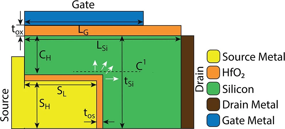
DLES-TFET
tunnel field effect transistor
Dopingless extended source tfet for switching and analog/RF applications
A doping-less extended source tunnel FET (DLES-TFET) is proposed for low power switching and analog/RF applications. In the proposed structure, the source metal is extended into the intrinsic Si-channel to form p+-source using charge plasma. An n+-drain is created by inducing electrons from drain metal to intrinsic Si-channel. Further, the gate metal in DLES- TFET is extended towards drain to obtain a field plate structure which improves the performance of proposed device. The performance of the proposed DLES-TFET is investigated using 2D simulations in TCAD tool (ATLAS). Our simulation results reveal that the DLES-TFET achieves high ION /IOFF of 2.86 × 10¹³, low subthreshold swing of 1.5 mV/dec and low threshold voltage of 0.24 V. Additionally, suggested device attains a peak transconductance of 115 µS/µm, cut-off frequency of 33.3 GHz, and offers a gain bandwidth product of 15.2 GHz.
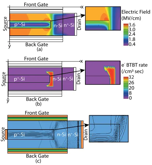
ESDG-TFET
tunnel field effect transistor
Extended-source double-gate tunnel fet with improved dc and analog/RF performance
In this article, we propose an extended-source double-gate tunnel field-effect transistor (ESDG-TFET) to enhance the dc and analog/RF performance. The source of an ESDG-TFET is extended into channel to increase the line and point tunneling in the device at the source-channel junction. 2-D simulations in the TCAD tool (ATLAS) are carried out to analyze and investigate the performance of the proposed device. At optimized device structural parameters, the ESDG-TFET provides a low threshold voltage of 0.42 V, a low subthreshold swing of 12.24 mV/decade, and a high I ON /I OFF of 2.57 × 10 12 . Furthermore, the proposed device achieves a maximum transconductance of 238 μS/μm, a cutoff frequency of 37.7 GHz, and a gain bandwidth product of 3.4 GHz.
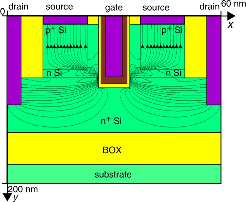
DCTG-TFET
tunnel field effect transistor
Dual-channel trench-gate tunnel fet for improved on-current and subthreshold swing
In this Letter, a dual-channel trench-gate tunnel field-effect transistor(DCTG-TFET) is proposed and investigated. The gate of DCTG-TFET is placed vertically in a trench to create two channels whichcarry drain current in parallel. The proposed device dimensionsare optimised to reduce channel resistance and tunnelling width foran appreciable increase in the ON-state current (ION). The performanceof DCTG-TFET is analysed using two-dimensional simulations inthe device simulator. The proposed DCTG-TFET provides one order of magnitude improvement in ION/IOFF current ratio and 17 timesreduction in subthreshold swing as compared to recently reportedtwo-source-region tunnel field-effect transistor structure.
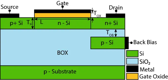
BBUD-TFET
tunnel field effect transistor
Controlling the ambipolar current in ultrathin soi tunnel fets using the back-bias effect
A two-dimensional (2-D) technology computer-aided design (TCAD)-based simulation study of the back bias in the ultrathin silicon-on-insulator (SOI) tunnel field-effect transistor (TFET) is presented. The transfer characteristics of a conventional TFET called the back-bias TFET (BB-TFET) depend on the back bias and the oxide thickness below the TFET epitaxial layer. The back bias affects the electric field at the source/channel and drain/channel junctions, hence both the ON-state current (ION) and the ambipolar current (IAMB) reduce with a negative back-bias voltage. This reduction in is not desirable in a TFET, hence a modified TFET structure called the back-bias underdrain TFET (BBUD-TFET) is proposed. In the BBUD-TFET, the back bias is applied on a p-Si pocket placed under the drain region, which is isolated using an ultrathin oxide. The back bias in the proposed BBUD-TFET mainly affects the electric field at the drain/channel interface, having a negligible impact on the source/channel interface. The BBUD-TFET structure is analyzed with or as the gate oxide. In the BBUD-TFET with as the gate oxide, the back bias completely suppresses the ambipolar current without reducing. Furthermore, the oxide thickness and back-bias voltage are optimized for the BBUD-TFET structure. In this study, 2-D TCAD simulations are carried out to investigate and analyze the performance of the BB-TFET and BBUD-TFET.
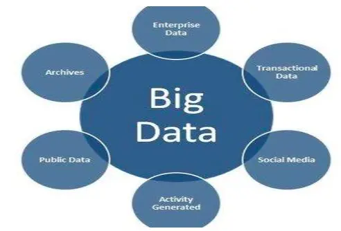
Big data for central banks
Big data for central banks: Exploring applications in monetary policy, financial stability monitoring and bank supervision
With the rapid adoption of artificial intelligence (AI) and big data analytics across high-impact domains like finance, healthcare and public policy, there are rising concerns about inadvertent biases and discrimination arising from opaque algorithms. Several instances have already emerged of AI systems unfairly disadvantaging minorities, women and vulnerable social groups due to historical biases in data, poor choice of proxy variables, narrow optimization objectives and lack of diversity. Addressing this critical issue, the field of algorithmic auditing has emerged to provide testing methodologies that can uncover harmful biases in AI models by auditing the entire pipeline from data collection to model development and deployment. Algorithmic auditing combines techniques like causal inference, adversarial testing, counterfactual explanation, and meta-learning to assess model fairness, explain model predictions, detect bias in training data and ultimately redesign systems to mitigate sources of unfairness. However, realizing the potential of algorithmic auditing requires overcoming key challenges around limited transparency of proprietary models, unrepresentative datasets, interpretability versus accuracy tradeoffs and the need for multidisciplinary teams combining technical and social science expertise. Further work is also needed on organizational aspects like developing auditing frameworks tailored to different application domains, integrating audits within model development workflows, and coordinating audits across stakeholders involved in AI systems. Overall, algorithmic auditing is a promising paradigm but still in nascent stages. Advancing frameworks, best practices and inclusive governance models for auditing will be crucial to steer AI systems towards fairness and address the growing risk of algorithmic biases.
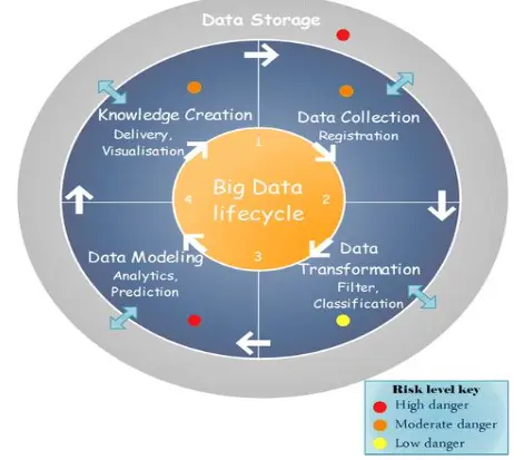
Privacy in IoT
Towards a secure and ethical framework for big data privacy in the internet of things (IoT) landscape
InThe proliferation of Internet of Things (IoT) technologies across various sectors such as healthcare, transportation, and smart cities has exponentially increased the generation of big data, elevating concerns related to data privacy, security, and ethics. This research study aspires to address these critical challenges by conceptualizing and developing a comprehensive framework specifically designed for the secure and ethical management of big data in the IoT landscape. Adopting a multi-faceted methodology that combines an exhaustive literature review, theoretical modeling, cryptographic algorithms, data anonymization strategies, and ethical compliance measures, the study introduces an innovative framework. This framework is rigorously validated through empirical case studies involving real-world IoT deployments in healthcare and smart home environments. The evaluation demonstrates substantial improvements in data privacy and security while maintaining strict adherence to ethical guidelines. The findings have far-reaching implications for multiple stakeholders, including IoT device manufacturers, software developers, data scientists, and policymakers. The study thus underscores the urgent need for a balanced, robust approach to big data privacy and ethics in the complex, interconnected realm of IoT technologies.
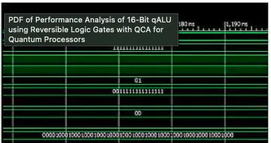
16-bit qALU
Performance analysis of 16-bit qalu using reversible logic gates with qca for quantum processors
he NAND, NOT, and NOR logic gates which are utilised to realise the hardware modules of the system, are examples of basic classical logic gates that make up the hardware basics of electronic circuit systems. In addition to this, a useful system has been described for designing and implementing quantum processors by using reversible logic gates to analyse the performance of ALUs. Additionally, it shows that QCA might be used in quantum computers, assuming that the underlying technology can be made workable. When considering energy-efficient computations, reversible or information-lossless circuits are crucial for digital signal processing, communication, computer graphics, and cryptography. By preventing information loss, reversible logic is utilised to lessen the power dissipation that occurs in classical circuits, which is particularly promising because it allows for extremely low power computations like nano-computing for quantum processors. Because bits of information are lost during logic operations, typical digital circuits waste a lot of energy. It is well known that an Arithmetic and Logical Unit is one of the most fundamental operational units in the quantum processor (ALU). The design and implementation of an innovative r/q 16-bit ALU that improves the overall performance of quantum processors while carrying out the task in the digital signal processing domain are discussed in this study. When reversible gates were used in place of logic gates, the power dissipation in terms of information bit loss was significantly reduced. Simulation of these circuits is done by QCA Designer tool and language used for programming is very high-speed hardware integrated circuit hardware descriptive language, Verilog HDL. The power and delay analysis of the various sub modules is performed and a comparison with the traditional circuits is also carried out. The designed ALU has better efficiency as it has less power loses and reduction in power loss upto 39 % is obtained.
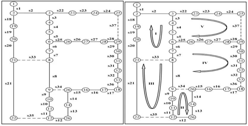
Optimizing DGs
Optimum placement and sizing of DGs using optimization techniques and distribution system reconfiguration
This paper presents Distributed Generator (DG) sizing and placement problem and reconfiguration of distribution system using optimization techniques. For the DGs sizing and placement problem, the main procedures are identified, studied and analyzed. Works of different authors are reviewed to gain the basic knowledge of the problems. In the paper, the advantages of DG implementation are observed. Here the loss reduction of the distribution system is taken as the main objective function. To find the optimal result of this objective function, differential evolution (DE) and particle swarm optimization with extermal optimization (PSO-EO) techniques are used. In the second work, reconfiguration of the distribution system is executed by changing the statuses of sectionalize and tie switches of the system. Using differential evolution (DE) optimization technique, different switching combinations are created. Here the main objective is to minimize the loss of the system and find the best configuration of the radial distribution system.

